Products
What is solar cell? |
|
A photovoltaic cell (commonly called a solar cell) is a nonmechanical device usually made from silicon alloys. It converts sunlight into electricity. The PV cell was discovered in 1954 by Bell Telephone researchers. Late 1950s, PV cells were used to power U.S. space satellites. Individual cells can vary in size from about 1 cm to about 10 cm. Most photovoltaic cells are about ten percent efficient in covering sunlight to electricity with further research being conducted to raise this efficiency to fifteen-twenty percent. Photovoltaic conversion is useful for several reasons. Conversion from sunlight to electricity is direct, so that bulky mechanical generator systems are unnecessary. The modular characteristic of photovoltaic energy allows arrays to be installed quickly and in any size required or allowed. Presently BCSC (Buried Contact Solar Cells) and Polycrystalline CdTe-baser Photovoltaic are the latest technology in the solar cells and having efficiency is around 16-22 % approx. and we can get stable power output and long life. |
How does a solar cell work? |
|
Sunlight is composed of photons, or particles of solar energy. These photons
contain various amounts of energy corresponding to the different wavelengths of
the solar spectrum. When photons strike a photovoltaic cell, they may be
reflected, pass right through, or be absorbed. Only the absorbed photons provide
energy to generate electricity. When enough sunlight (energy) is absorbed by the
material (semiconductor), electrons are dislodged from the material's atoms.
Special treatment of the material surface during manufacturing makes the front
surface of the cell more receptive to free electrons, so the electrons naturally
migrate to the surface. When the electrons leave their position, holes are
formed. When many electrons, each carrying a negative charge, travel toward the
front surface of the cell, the resulting imbalance of charge between the cell's
front and back surface creates a voltage potential like the negative and
positive terminals of a battery. When the two surfaces are connected through an
external load, electricity flows.
|
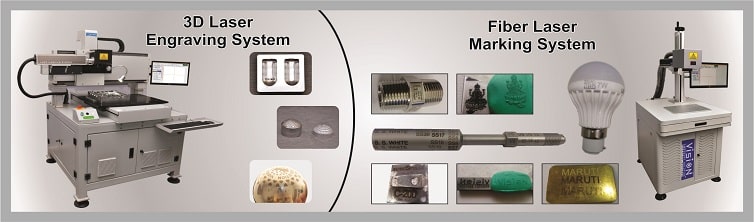
| What is scribing and why scribing is necessary? |
|
Scribing means, cutting of a grid pattern of grooves in a semiconductor material
generally for the purpose of marking interconnections or to cut the solar cells
into two parts. Laser scribing is done for the fabrication of monolithic cell interconnections. Scribing, either with a mechanical stylus or a laser is used for fabricating series interconnections allowing a large, thin-film photovoltaic panels to be made with, for example, 100 cells monolithically interconnected. The series interconnection allows the same electrical power to be produces from the panel with a voltage 100 times that of an individual cell and the current equal to that of one cell. For CdTe thin films, the individual cell voltage is about 0.8V |
| Laser Type | Fiber Laser |
|---|---|
| Laser | Fiber Laser,Diode Pump, Nd:YAG Laser |
| Average /CW Output Power | 20 W |
| Pulse Repetition Rate | 20-80 KHz |
| Wavelength | 1062 ± 3 nm |
| Laser Class | IV |
| Guide Laser/Red Aiming Beam | Yes |
| Ambient Temperature | 25 °C |
| Power Consumption | < 1 kW |
| Electrical Connection (Optional) | 230v/50Hz - 115V/60Hz |
| Axis Travel (Optional) | 200 x 200 mm /250 x 250 mm |
| Repeatability | 50Micron |
| Resolution | 1micron |
Contact us +91 7575806266 Email : sales@vesindia.org, bhavesh.pethani@gmail.com


| Home | Business Profile | Products | Blog | News | SiteMap | Contact Us | About Us
